Products...
Products
Our Products
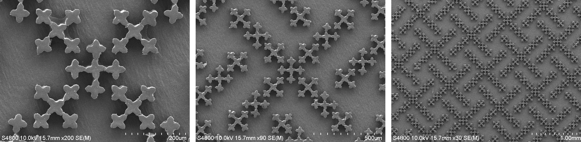
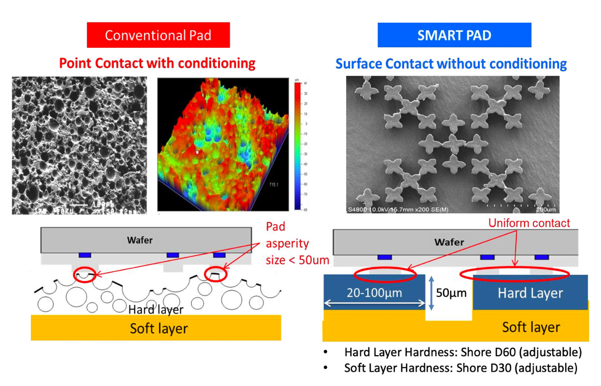
SMART PAD’s revolutionary CMP pads are composed of customizable non-porous microstructures on the surface of the polishing pad and an elastic sub-layer. These application specific/tunable features provide uniform contact up to 20% of surface area to the wafer, and improved slurry retention.
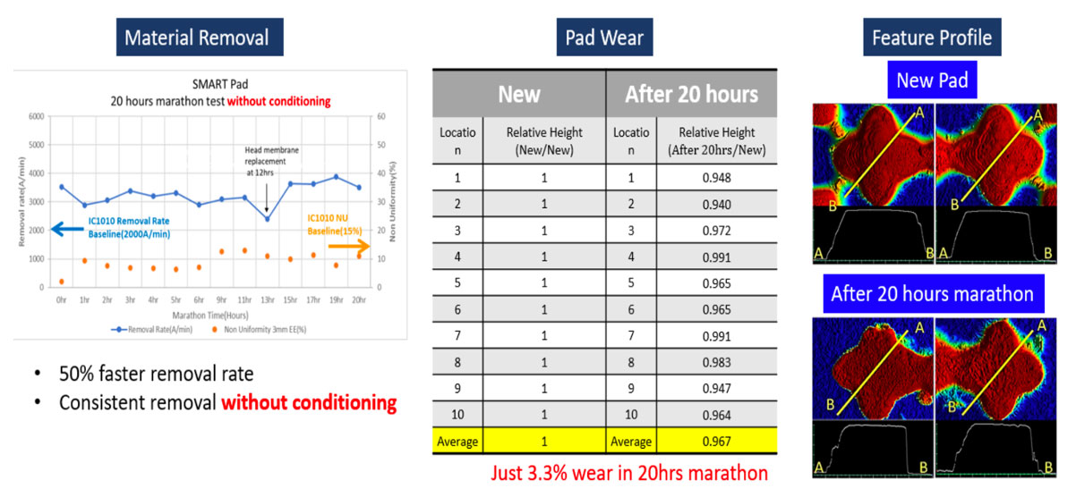
Our pads will significantly improve removal rate, planarization, and uniformity as well as minimize pad deformation during polishing, therefore, will eliminate the pad conditioning process. Semiconductor companies can save millions annually by adopting SMART PAD.
Problem Statement
As the design rule of the semiconductor-chips become sub-5nm, it has become extremely difficult for the chipmakers to secure acceptable production yield. As one of key chip-manufacturing processes, Chemical Mechanical Planarization/Polishing (CMP) process has also faced tighter process margins such as higher polishing speed, lower scratches, and greater planarization efficiencies (flatter post polishing surface in a given time). Cost reduction is also very important for the chipmakers.
Solution
Conventional polishing pads for CMP are like polyurethane sandpapers which have random asperities. Whereas, SMART Pad’s polishing pads have engineered polyurethane micro-structures on the pad surface, providing much more efficient and precise polishing performance as well as tunability to the end-users. Another key advantage of SMART Pad is that customer can eliminate one of their CMP consumables with our products, resulting in huge cost saving.
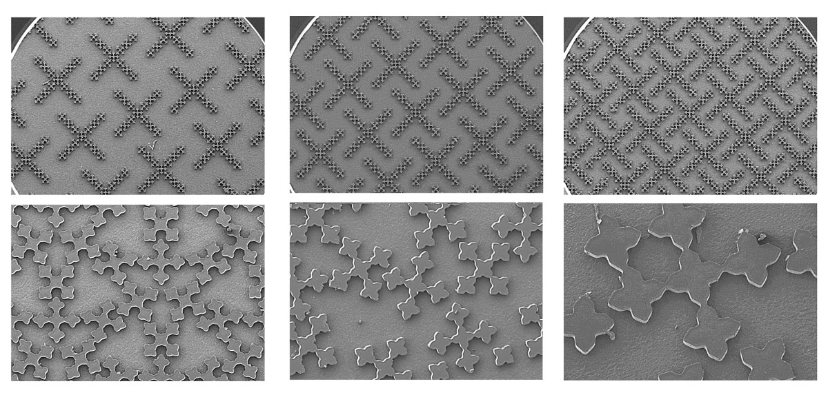
Customizable Design
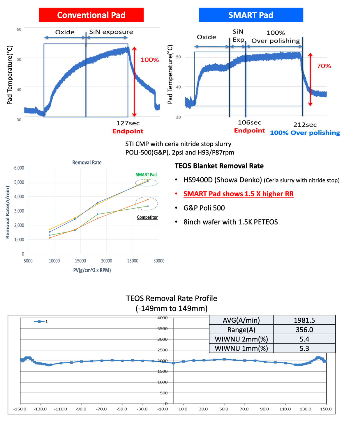
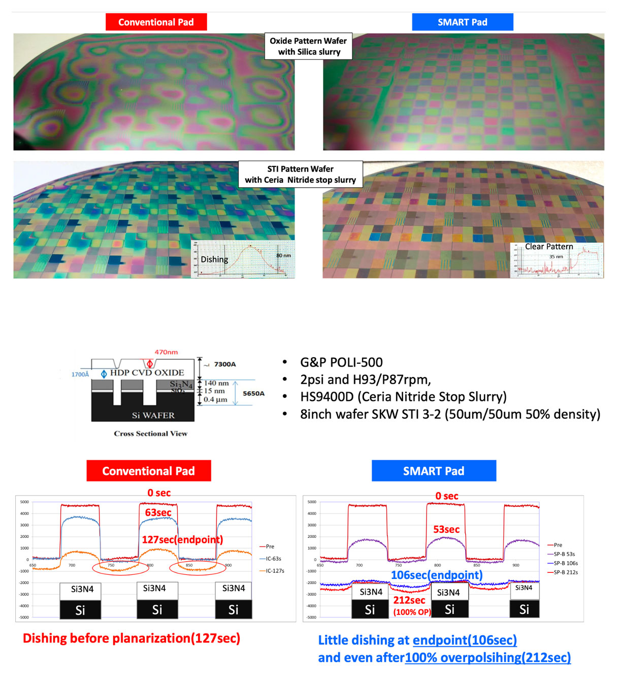
Test Results
According to our initial tests and customer’s feedbacks, our products perform superior to the conventional pads at advanced CMP process which requires complicated polishing and stopping mechanism.